If you’re as old as I am, one of the coolest toys in the 1960s was the Viewmaster 3D “stereoscope!” Before we all had personal computers and cell phones, we’d insert special photo “disks” into the handheld viewer and see things in three dimensions … How cool is that?!
At Silicon Forest Electronics, we now utilize the benefits of 3D technology in our manufacturing and quality assurance processes:
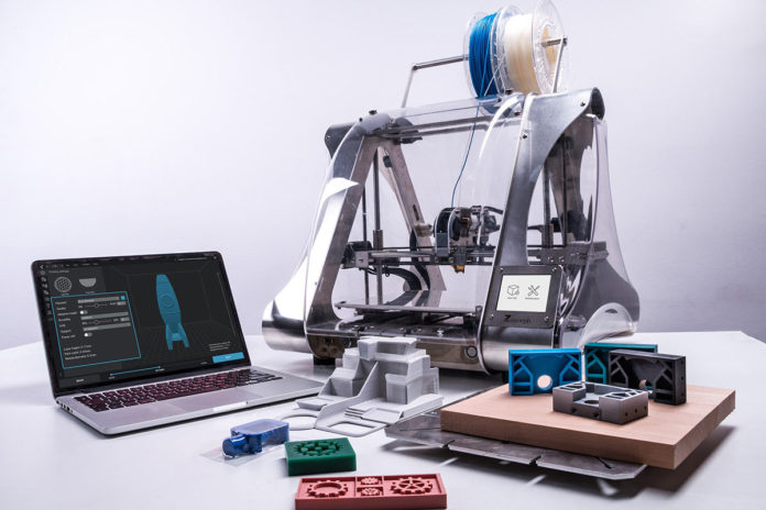
3D Printing is a new and exponentially growing technology that seems to have hit everyone like a large sack of bricks. It is being used all the way from small-time hobbyists to some of the biggest corporations in the world. We use this technology to save on the cost of fixtures that in the past needed to be produced at a machine shop. Not only does this save on the initial cost for creation, but as many people know nothing is ever perfect the first time and repeated revisions is not something that comes cheap at a machine shop. Not to mention the lead time of building the fixture in house and the fact that one of our engineers gets to play in SolidWorks just makes this even more appealing.
3D Solder Paste Inspection (SPI) is a process that was developed to provide accurate measurements of every solder paste deposit on a printed circuit board BEFORE any components are placed. 3D SPI systems do it very fast; inspection speeds for some of the newer systems commonly achieve hundreds of solder paste deposits per second, meaning that these systems will never bottleneck the line. Real-time quantitative data from these systems makes process analysis easy and trends (good or bad) become apparent very quickly via integrated statistical process control software.
3D Automated Optical Inspection (AOI) was developed to address the limitations of traditional 2D (two-dimensional) AOI systems. While 2D systems use multi-colored LED lighting and high resolution cameras to inspect components and solder joints, these systems rely solely on reflected lighting and are not ideal in certain cases where solder joints are particularly shiny or when accurate detection of slightly lifted component bodies and/or leads is required. 3D AOI systems were developed to address these limitations.
X-ray inspection in the electronics industry is a process that has been around for a long time, starting with simple 2D radiography. In recent years, the capabilities of X-ray equipment has skyrocketed for electronics due to more and more complex assemblies, where 2D X-ray inspection is no longer feasible for certain components. With our 3D X-ray system, we can automatically check whether or not a solder joint meets requirements, in fact, now we probably know more than we would ever want to know about those solder joints. Qualification of our 3D X-ray has been completed and it is currently being used for inspection on our production lines.
As cool as it was, we’ve come a long way down the 3D technology road since the Viewmaster!
Jay Schmidt is executive vice president/general manager at Silicon Forest Electronics. He can be reached at jay.schmidt@si-forest.com. Chief Technology Officer Kevin Syverson and Process Engineer Colin Campbell also contributed to this column.


